This work want to show
the validity of Lock In modulation in ULF (0.1-30Hz Ultra Low Frequency)
receiver application. Transistor, vacuum tubes, resistor and other devices
exhibit a low frequency phenomenon know as flicker noise, often called
1/f noise because the mean square density is proportional to 1/fvv
» 1. Flicker noise pose serious problems for low frequency application
but Lock In modulation could be the answer.
Theory of Lock
In Modulation and Demodulation
|
|
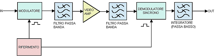
The synchronous mod/demod is also called Lock In
modulation (Fig.1). It is a modulation on a different frequency from the
original signal, to transfer out of 1/f noise
(fig.2), where is prevailing the instrumental noise or pink noise. This
frequency is knowing like fchopand
it must be upper knee frequency fknee
(Fig. 2), where we have the crossing from 1/f
noise region to white Gaussian noise region.
 |
The Lock In modulation is also calling Chopping modulation, in fact it using Chopper amplifier.
We know that translate a signal in frequency is like to sample it, Lock In modulation is like a sampling at Fc frequency, we have for Nyquist theorem, that Fc must be twice of maximum frequency of the signal.
The action consist to select the interest signal, modulate ,enlarging, filtering with a pass band filter and demodulated synchronous with the modulator.
The demodulated signal will be enlarging to obtain a signal noise ratio S/N >1 . We have the advantage that all the offset and the drift produces inside the Lock In are banishing here.
Now we can see the frequency answer of a Lock In
system with a time variant signal:
| V0 cosw1
t
Signal In
A cosw0 t Synchronous Reference |
Where w0 is chopping pulsation and w1 is the fundamental pulsation.
The demodulated signal is:
![]()
We have Dsb-Sc (Double Side Band Suppressed Carrier) spectrum, looks like an AM spectrum without the unmodulated carrier impulse, the information is in the double side band (Fig 3).
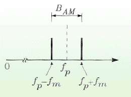
Picture
3 - DSB-SC Spectrum
Synchronism in Lock In Modulation.
The synchronism in Lock in modulation/demodulation is one of the most recurs technical problem. In fact we must to give a very synchronous signal to Modulator and Demodulator. Often the cause of the asynchronism is the different propagation time from the synchronous signal generator and the modulator/demodulator devices .
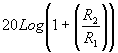
The importance of a very synchronous reference is given from the fact that a phase difference f from signal to demodulate and the synchronous reference will give an error on the continuos component; this error is estimated to be:
![]()
with: 0<?<90
the wave form are in Fig. 4
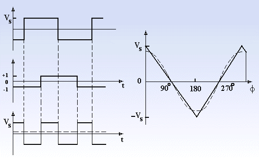
Picture
4 - Amplitude and phase with asynchronism
The demodulated signal, for the phase displacement have a smaller amplitude. We can see that the amplitude is inversely proportional to the grow of phase difference. In particularly we have the signal annulment at 90° and his multiples, where the demodulated signal is not present. For the odd multiples of 180° we have an inversion of the sign
ANALOG DEVICE AD630 Balanced Modulator-Demodulator
We have choose for our examination the Analog Device
AD630. Its a high precision balanced modulator which combines a flexible
commutating architecture with the accuracy and temperature stability. Its
signal processing application include balanced modulation and demodulation
, synchronous detection ,Lock in amplification and square wave multiplication.
Its works like a precision Op amp with two independent differential input
stage and a precision comparator which is used to select the active front
end. (Fig 5)
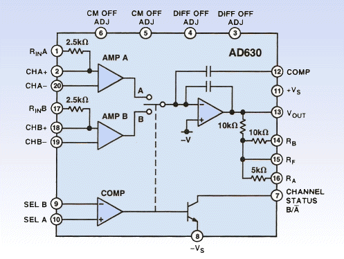
Picture
5 - Functional block diagram.
Lock In amplification is a technique which is used to separate a small, narrow band signal from interfering noise. Very small signal can be detected in presence of large amounts of uncorrelated noise when the frequency and the phase of the desire signal are known.
Our experiment consist to realize a Lock In ring with two AD630, one like synchronous Modulator and one like synchronous Demodulator
The data sheet says that AD630 could be recover a small signal from 100 dB of interfering noise at 1 Khz, we want to verify if is possible to recover small signal from noise at 100 Hz.
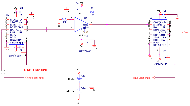
Electric circuit
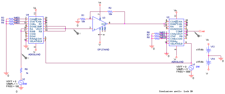
Picture
6 - Wiring diagram
We have pointing our attention around U.L.F. (0.1¸
30Hz) and we have chose a center frequency of 100 Hz for our simulation..
| Input signal | Offset | Freq. | V.ampl. |
| Sin | 0V | 100 Hz | 0.1-5V |
| Modulated signal | Offset | Freq. | V.ampl. |
| Sin | 0V | 1 KHz | 5V |
Between modulator and demodulator there is an Op amp to enlarge the signal , the Op amp chosen is the Analog Device Op 27 . It must to guarantee a large gain bandwidth represented by:
![]()
where G is the gain and B the band of applicated signal. For OP27 the gain bandwidth is about 8 Mhz ; we can have good gain (100, linear) for a signal with 100 Khz band. Last but not least the OP27 have a very good noise figure.
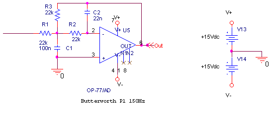
Filtering of output signal
The modulation of a signal by a sinusoidal wave
generate some harmonic at nfs,
(for us f = 1kHz frequency, for this reason
after demodulation the signal must be filtering with a LPF (low pass filter).
The output low pass filter is a 2nd order Butterworth with Ft=150Hz:
| OPAmp. | Approx | Order | Ft | Gain | Config. |
| OP77 | Butterworth | 2° | 150Hz | 1 | Invertente |
 |
Now we start to simulate by PspiceÒ , all the Lock In ring. We have to add to input signal (Test signal) a white gaussian variable noise source, than modulated by AD630 enlarging by OP27 and demodulate by AD630. We have to vary the test signal amplitude and to verify the correct recovering of the test signal from varied dB of interfering noise.
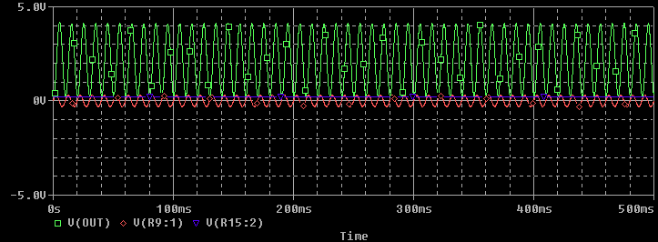
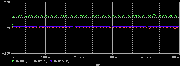
In the follow table the most important result:
| Vin
|
Vnoise
|
Sign/Noise
|
GAmp
|
Demod. | Simulazione:
Red=Input 100 Hz Green=Out Demodulated |
|
| 1V | 1.26 |
-2 dB | 6 dB | Yes | ||
 |
||||||
| 0.3V | 1.90 |
-16 dB | 20 dB | Yes | ||
 |
||||||
| Vin
|
Vnoise
|
Sign/Noise
|
GAmp
|
Demod. | Simulazione:
Red=Input 100 Hz Green=Out Demodulated |
|
| 0.1V | 1.26 |
-25 dB | 27dB | Yes | ||
 |
||||||
| 0.01V | 1.26 |
-40 dB | 40 dB | Yes | |
 |
|||||
| Vin
|
Vnoise
|
Sign/Noise
|
GAmp
|
Demod. | Simulazione:
Red=Input 100 Hz Green=Out Demodulated |
|
| 0.01V | 1.90 |
-45 dB | 46 dB | No | ||
 |
||||||
The PspiceÓ simulation given some important result, we cant confirm the Analog Device result obtained at 1 Khz but we could be satisfy for our -45 dB (S/N [dB]) at 100 Hz.
The PspiceÓ simulation is limited by the white gaussian variable noise source, we must to create a "ad hoc" device to generate suitable noise because in PspiceÓ dosnt exist one.
Now we pass to realize really the same circuit simulated
by PspiceÓ
. The wiring diagram is at Fig. 7 , we want to find a confirmation at what
we have simulate
 |
The circuit was made on a Bread Board , (Fig. 8).
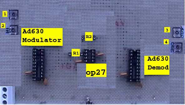
Picture
8 - Components on the Bread Board
On the Bread Board we have four In/Out gate at 50 Ohm SMB connection.
1: NOISE: Input from noise generator
2:INPUT: Input 100 Hz test signal.
3:OSCILLATOR: Synchronous reference for Modulator-Demodulator at 1 Khz
4:OUTPUT: Output of demodulated signal.
There is a dual power supply tower +15V 15V too.
We have test every single circuit components and then all Lock In ring.
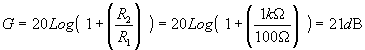
The not-inverted OpAmp OP27 gain is:
The INPUT test signal was a 100Hz and the amplitude
was varied from 500mV to down.
Then we varied noise source intensity and the test
signal amplitude to verify correct recovering of the test signal.
We have verify the correct recovering of signal until:
![]() .
.
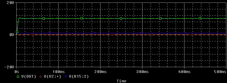
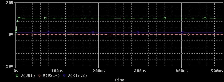
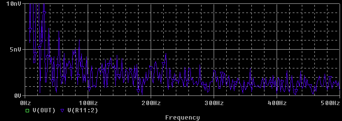
The oscilloscope wave form are at Fig. 9, on the 1st channel there is the modulated signal at 1 Khz, on the 2nd channel the test signal correctly demodulated. and enlarging.
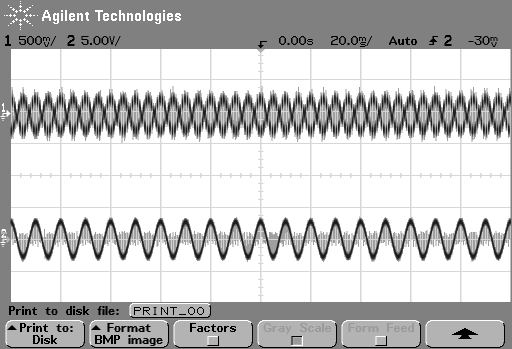
Picture
9 - Modulated Vs Demodulated
The zoom of the oscilloscope wave form are in Fig.10 and Fig. 11.
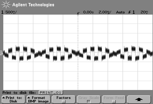
Picture
10 - Zoom of Channel 1
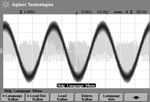
Picture
11 - Zoom of Channel 2.
The object of our work is to find the maximum signal noise ratio (S/N) where the signal is correctly recovery
The Analog device Data Sheet give a border of 100dB a 10 Khz.
The PspiceÓ simulation confirming the superiority of Lock In modulation for U.L.F. application and give a 45dB (S/N).
The carrying out of the circuit and the simulation havent permit to confirm the result of the software, we can recovering monochromatic signal only until
(S/N) < -20dB.
The experimental result is the worst but is at the same time more interesting.
In fact the recovering of small signal in U.L.F band with (S/N) < -20dB is a great result impossible to obtain with other technical devices.
Another part of this works and some application are on line at www.qsl.net/iw2lla.
Thanks a lot to Ing. Jader Monari andIng Marco Poloni from Istituto di radioastronomia CNR (Italian National Research Council ) of Medicina (Bo) and Ing. Stelio Montebugnoli general manager of the istitute .
Bibliografy:
C. Vignali (I4VIL):Radio Rivista 10/2002-Ricevitori a rivelazione Sincrona
F.P.Panter:Modulation-Noise and Spectral analysis Mc Graw Hill 1985
Monari-Guidi-Poloni : Circuito di riferimento per
Mod/Dem Lock In
Marco Poloni: Tesi di Laurea
Analog Device AD630 Data Sheet
Author:
IW2LLA Dott. Ing. Andrea Ghedi
Andrea GhediÒ
2003 Publication only for ham and no profit use.