A 0.1 to 40 Hz SENSING,
CONDITIONING AND RECORDING SYSTEM

Part 2/3 : the signal conditioner

By Serge Lacôte (France)


The signal conditioner
After picking up and preamplifying the ELF signal, it's necessary to re-amplify it again and filter it to eliminate uninteresting and harmful frequencies, i.e. higher than 40 Hz, specially the omnipresent 50 Hz (or 60 in the USA) and, if possible, all the signals carried by power lines, signals which are often more harmful than the 50 Hz itself. The system here described consists of :
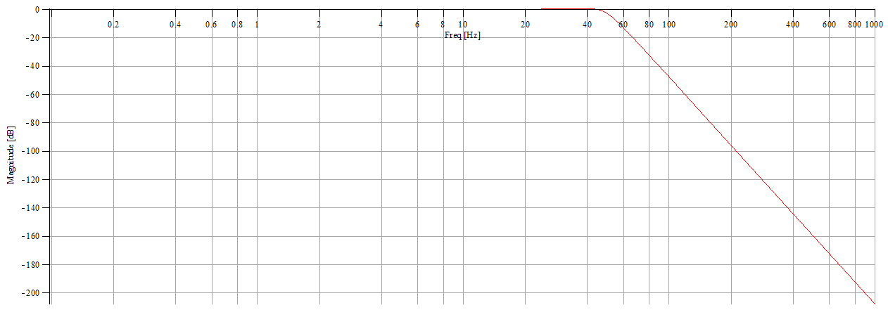
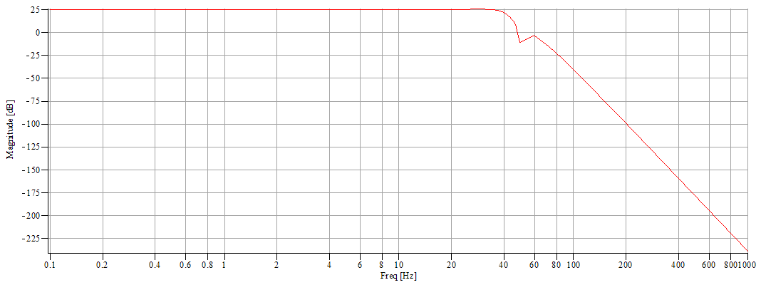
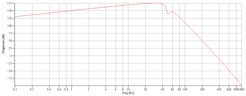
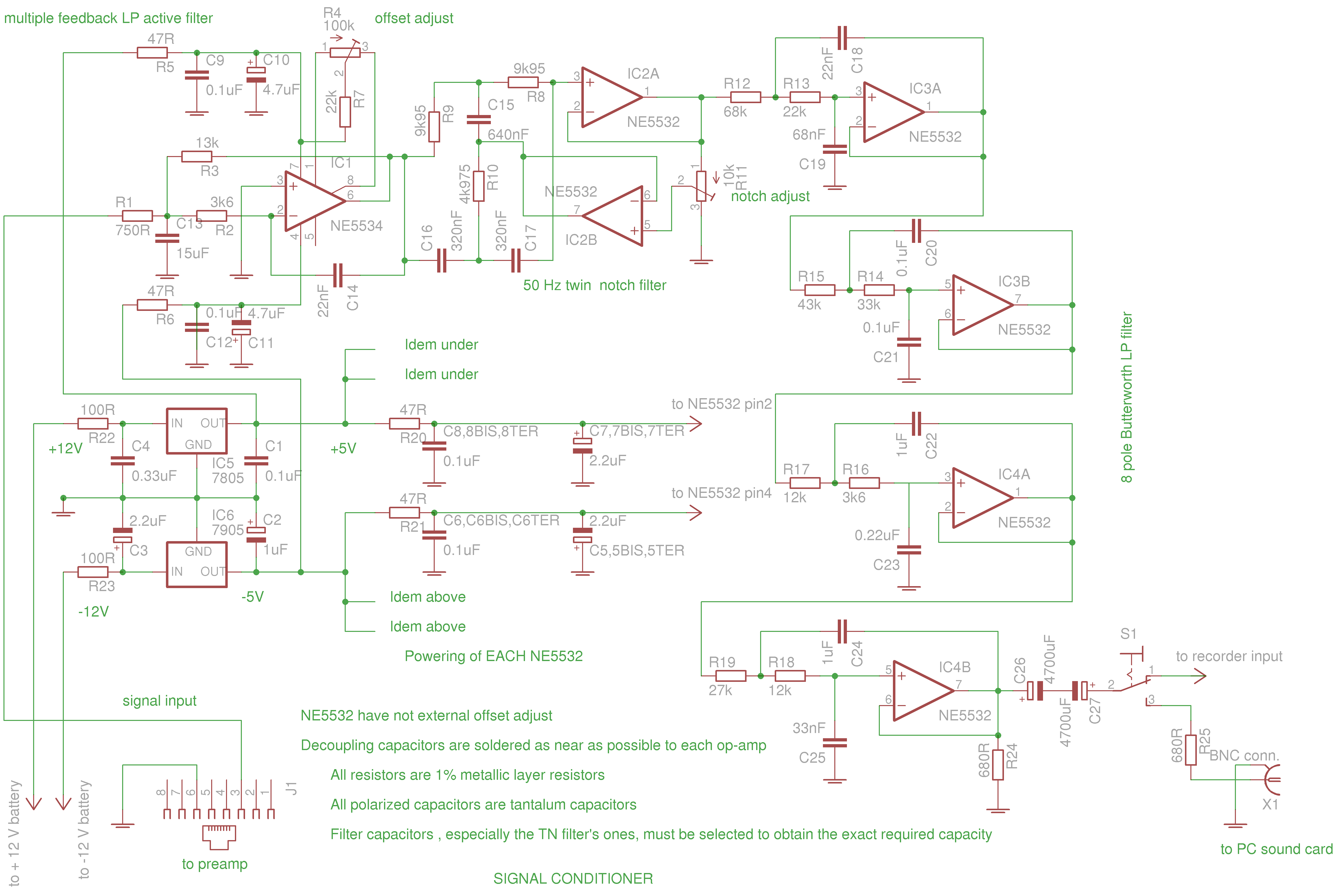
1°/ A multiple feedback active low-pass filter with a gain of about 18, a 40 Hz cutoff frequency and a quality factor of 2.2. This stage uses a NE5534 low-noise OP-AMP (less expensive than the AD797 used in the preamplifier).
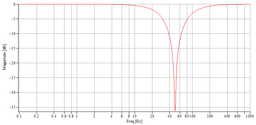
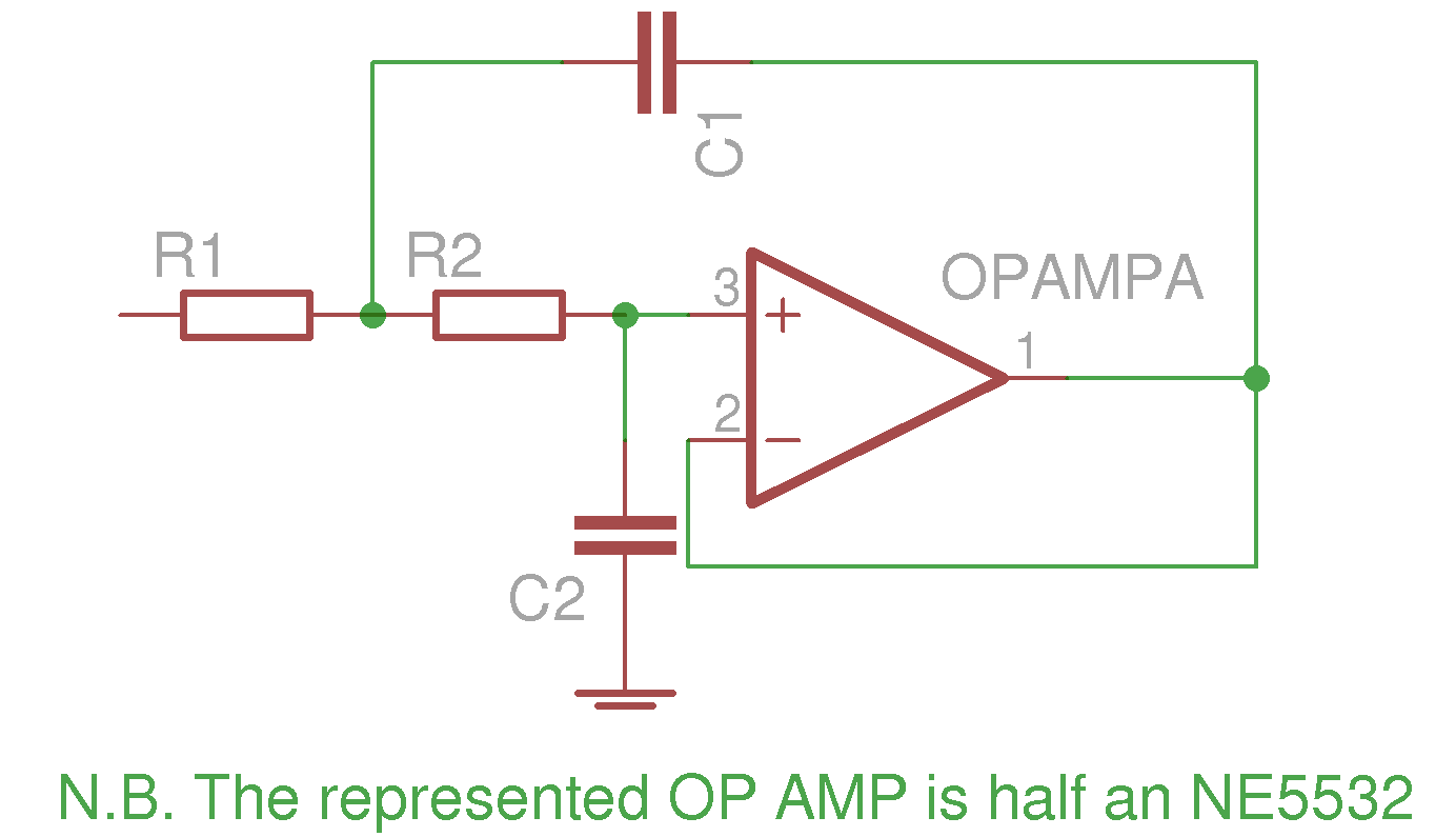
2°/ A 50 Hz active twin T notch filter using a cheap (but still good) double OP-AMP NE5532
3°/ A 8 pole Butterworth Sallen-Key active 50 Hz low-pass filter using two NE5532s.

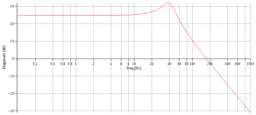
N.B. These specifications were determined after multiple trials at the same time making trial graphic transfer function simulations and some concrete implementations. The difficulty was to obtain a relatively horizontal response curve between 0.1 and 40 Hz and a drastic drop after 40 Hz. I have finally chosen not to totally crush the 50 Hz to obtain a frequency reference line on the spectrograms and to be able to control the recorder sampling rate. It's evident that it's possible to make different choices and obtain better or different results. The calculation details of components values is provided in order to build a system with other bandwidths, such as 0.1-5 Hz or 0.1-120 Hz. For this purpose, the recorder sample rate was fixed at a relatively high value to be able to change filter characteristics without changing the MCU programmation (see part 3). Regarding that, remember that the preamplifier contains a primary filter with a 87 Hz cutoff frequency and it might be necessary to change the C9 value (see part 1).

The outpout signal may be sent to a PC sound card used as A/D converter to allow real time FFT analysis, a very useful option for the developement, or to the recorder, which is the normal system using mode. 


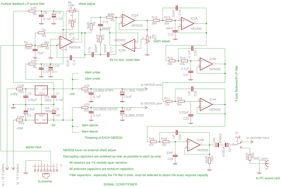
Click here for a full resolution scheme

For the filters calculation (and using OP-AMP) I have mainly used Chapter 8 of the Analog Device study named Analog Device Basic Linear Design (ADBLD), which is freely downloadable on the AD site and the Texas Instruments study named Active Filter Design Techniques. A dual 5 V power supply is used, but 3.3 V would suffice. The 2350 uF coupling capacitor C26+C27 is indispensable when the system is used with the recorder. The sound card impedance adaptation R25 does not have any absolutely critical value but its presence is necessary.
There now follows the calculation details using Maple 14 (but any calculator will do).


The multiple feedback low pass filter design.

For capacitors and resistors I am keeping the names of the above schematics. The other notations are :
: cutoff frequency ; ; : quality factor ; : damping ratio ; : signed gain at 0 Hz (obtained making s=0 in the transfer function ; here -18). Resistors and capacitors determine unambiguously precedent parameters but the reciprocal is false : for the determined choice of , there are a lot of possible choices for resistances and capacities. The theory shows that their values are linked by the following relations :
; ; . The problem consists of using capacitors and resistors whose values can easily be found and satisfy these relations. Considering the fact that , (value hoped) and , we have a system of 3 equations in 5 unknowns. The general solution will depend on two arbitrary parameters. Generally, we choose the capacities, but the system resolution shows that a certain discriminant must be positive. Here is my Maple worksheet :

>
>
>
(1)
>


(2)
>
(3)
>
(4)
>
>
(5)
>
(6)
>
(7)
>
(8)
>
>
>
>
>
(9)
>


(10)
>
>
>
>


(11)
>
(12)
>
(13)
>
(14)
>
>
>
(15)
>
(16)
>

>
>
(17)
>
>
(18)


We can see that pole real parts are strictly negative, as it is necessary.


The twin T notch filter

Capacitors and resistors names are those of the schematic. Here, for evident reasons, the components implemented values must be as near as the theoretical ones : 50 Hz is 50 Hz ! The other notations are :
: cutoff frequency, here 50 Hz ; ; quality factor ; I use the calculation method developed in ADBLD ch. 8, p. 8.101. We have and . We have ; there is no other equation to determine R and C and we can choose R or C. We can adopt 320 nF for C (in practice, is obtained by two 320 nF capacitors in parallel). It then results that (in practice, by testing different 10k resistors it is easy to find one ; is obtained by two 9k95 in parallel). The trimmer can be decomposed in connected to IC2 pin 1 and connected to GND. The and values determine the notch depth. We have (or ) and there is no other equation to determine and . The sum is not critical and we can adopt 10 kOhms.
The transfer function is 
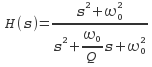
i.e. , if we set the trimmer so that , which corresponds to the best experimental result : .

Pole calculation :


>
>
>
>
(1)
>
>

>
>
(2)
>
>
(3)
>


The 8 pole 50 Hz Sallen Key Butterworth low-pass active filter

Capacitors and resistors names are those of the schematic. The other notations are : : cutoff frequency, here 50 Hz ; ; quality factor of each considered stage. This filter is constituted of 4 second order Sallen Key stages in cascade. The characteristics of these stages must respond to a precise layout if we want to have a true 8 pole Butterworth filter. The parameters of each stage are consigned in an array like the one p. 8.42 ch. 8 ADBLD. It's possible to impose the poles or, besides the cutoff frequency, the quality factor Q. We adopt the last way. The Q factors of different stages must be :

stage

1

2

3

4

Q

0.5098

0.6013

0.9000

2.5628


The generic schematic for a second order Sallen-Key low-pass filter with a gain equal to 1 (0 dB) at the origin is :


The capacitors and resistors values are linked by the 2 relations : and . We have 2 equations for 4 unknowns. We will see that we can choose C1 and C2 (under a certain condition) for example and obtain R1 and R2 in function of C1 and C2. This is the Maple worksheet :


>
>
>
>
(1)
>
>
(2)
>

(3)
>
>
(4)
>
(5)
>
>
(6)
>
(7)
>
>
(8)
>
>
(9)
>
>
(10)
>
>
>
>
>
>
>


(11)
>
>


(12)
>
>

(13)
>
(14)
>
>

>
>
(15)
>
(16)
>
(17)
>
(18)


Finally :

stage

1

2

3

4

C1

0.1uF

0.1uF

1uF

1uF

C2

68nF

68nF

220nF

33nF

R1

22k

33k

3k6

12k

R2

68k

43k

12k

27k


Note that there is a large arbitrary factor in these values and that many other choices could be made. Theoretically, the order of the cascade stages in Butterworth filter implementation is not fixed, but it's better to observe the described order “ to avoid dynamic range problems”(1).


Global system behaviour

This is the global response of the system to a sinusoidal magnetic field (normal to the loop plane, i.e. when with the notations of part one). The global system gain is the module of the ratio between the outpout RMS voltage of the output conditioner and the magnetic field RMS intensity expressed in teslas. This gain, expressed in dB, is plotted in the last amplitude Bode diagram of the Maple worksheet.


>
>
>
>
>
>
>
>
>
>
>
>
>
>
(1)
>

>
>
>


We can recognize the slope below 40 Hz due to the frequency proportionality of the e.m.f. induced in the loop and to the importance of the resistive factor in the loop impedance (see part one). As it can be seen on the waterfalls, this drawback is of no great practical importance in the qualitative use of the system.

End of part 2

1) Magister dixit : Horowitz & Hill, The art of electronics, 2nd ed., p. 275.


Return to the main index of www.vlf.it