CONDITIONING AND RECORDING SYSTEM
Part 3/3 : the recorder
By Serge Lacôte (France)

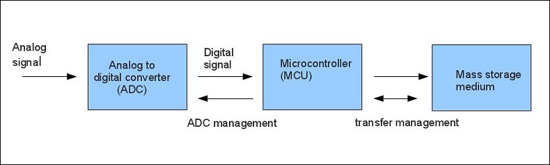
General architecture of the recorder
The general architecture of the recorder is the following :
Numerical data of the project partly determine the ways to operate, although there remains some arbitrariness. I am presenting a realisation which works correctly, but which, of course, can be improved.
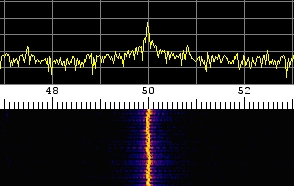
The Nyquist-Shannon sampling theorem imposes a sampling rate of at least 80 sps, but, for various reasons, I have fixed it at 128 sps, which being a power of two, is adapted to the FFT calculation with the Cooley-Tukey algorithm (even if the zero-padding tip allows escaping from this constraint). Furthermore, the 50 (60) Hz line is visible on the waterfalls, which enables a sample rate control.
A 16 bit resolution and a low noise level are required in order to lose nothing (or almost) of our weak signals picked up before with great pains.
All this leads us to turn to a successive approximation converter. I have chosen the Analog Device AD7680, the qualities of which are well-known. It is a non-differential input ADC, which accounts for its relatively low price, but requires refocusing the input signal, cleared of its continuous component, on Vcc/2 with a voltage divider and a large capacitor, which raises no problem.
The usual calculations related to the input calibration of an ADC are omitted here, for the reason that little is known about the conditioner output voltage, except that it is weak, at most some hundred millivolts. However, it is necessary to protect the ADC from transient peaks, as those produced by the unexpected passage of a car at a short distance of the loop.
Moreover, this smart ADC is kind enough to work with a 3.3V Vcc, which, so, may be the single supply voltage of all the recorder's ICs, the SD card included.
In connection with the chosen simplified operating mode (cf. infra Software architecture), a single midrange 8 bit microcontroller (MCU) is used to manage alternatively the sampling and the recording : the Microchip PIC18LF4620, which is the low voltage version of the PIC18F4620. A Maxim DS1302 real time clock (RTC) is associated with it to date recordings and a MAX3232 driver/receiver to debug the program and make various settings (date, time, recording time) with a PC linked to the recorder with a plain serial line.
The mass storage medium is a SD Card, which is at the same time unexpensive, convenient and easy to find. A 2 Go capacity is amply sufficient because, in view of the sample rate and the consumption of 2 Bytes per sample, a 24-hours' recording represent 24 x 3600 x 128 x 2 = 22118400 Bytes, i.e. about 22 MB. This size remains compatible with the venerable FAT16 file system, recognized by all computers and easy to use.
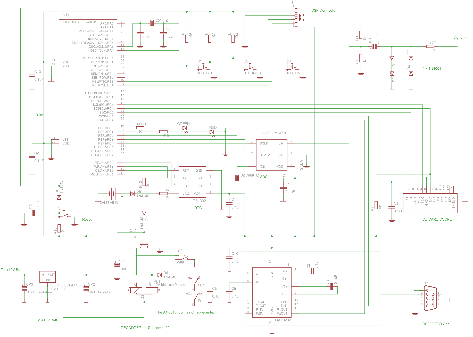
The schematics
Since the publication of parts I and II, I have brought some minor changes to the recorder, which are essentially:
- a. Two separate buttons to launch and stop the recording ("REC. ON" and "REC. OFF" buttons).
- b. An automatic switching off of the power supply after a recording error or after the recording is achevied.
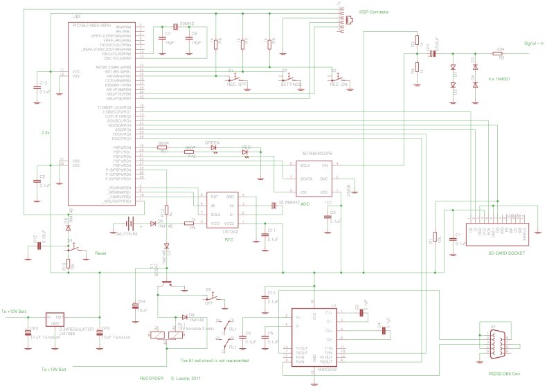
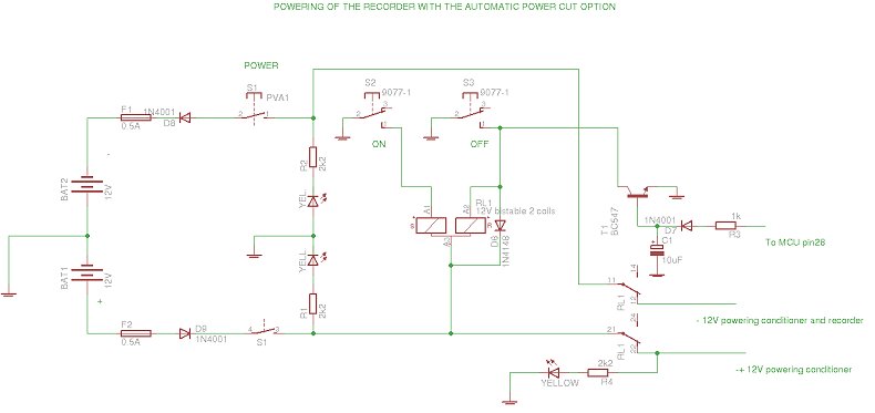
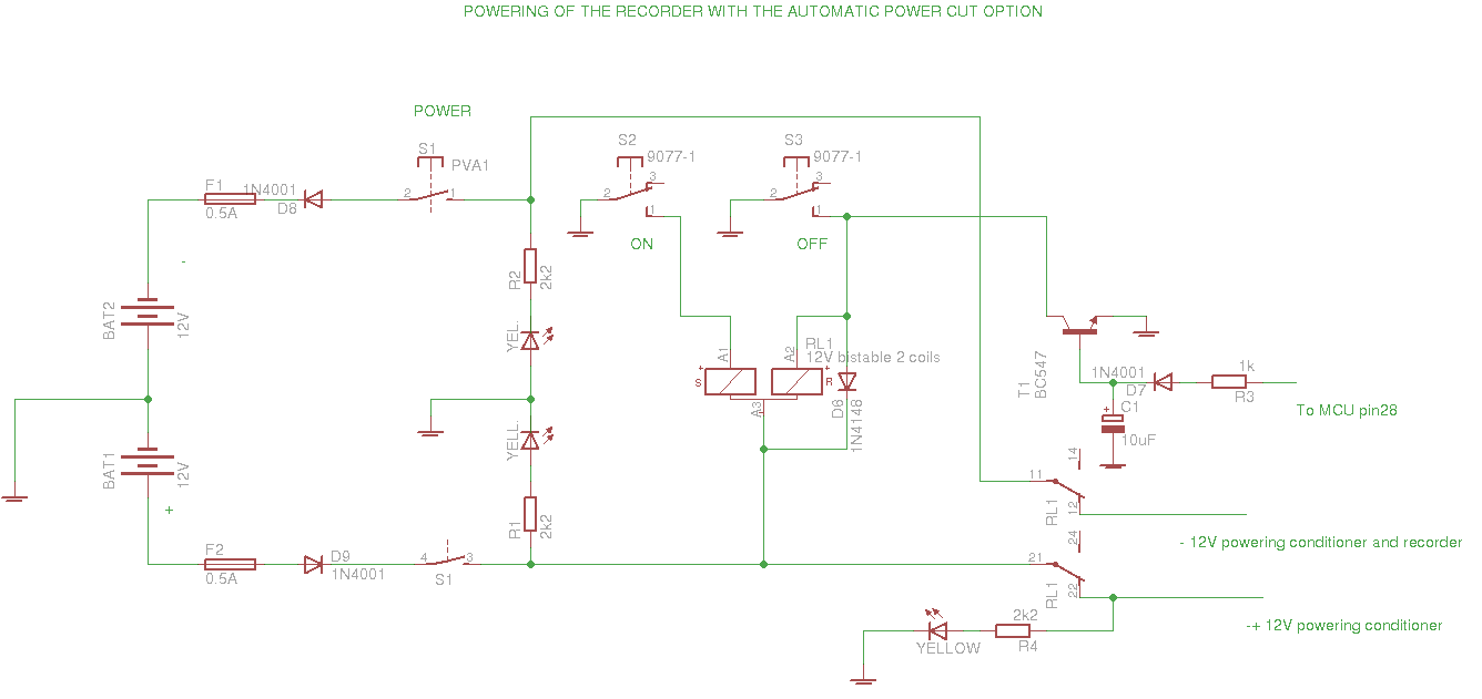
For a full resolution of the recorder schematic click here and for the powering click there
Comments about the schematics
Of course, the recorder schematic is designed in function of the chosen communication modes between the MCU, the card and the other integrated circuits. In our case, it is always the serial synchronous mode SPI (for Serial Peripheral Interface) that is used. This, in three places: between the MCU and the SD card, between the MCU and the ADC and between the MCU and the RTC. The communication with the PC, when it is requested, is asynchronous and uses the corresponding feature (EUSART) integrated in the PIC18LF4620. However, a driver / receiver IC (MAX3232) is necessary to adapt the signals to the RS232 norm. It is useful to know the principle of the SPI communication. Let's expose it briefly in the case of only one slave and a full duplex transmission.
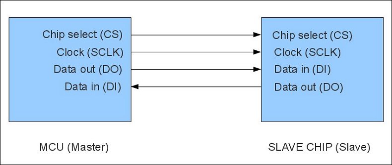
The wiring is very simple and reduced to 4 wires (even sometimes 3, as in the RTC connecting). To avoid confusions, which are very frequent, let's consider within this document that the reference is the master : for instance, DO means the DO pin of the master (which is linked to the DI pin of the slave), idem for DI.The beginning of a transaction is signified by the master to the slave by setting to 0 the CS pin of the master if the Idle is conventionally fixed to 1 (“Idle high”) or vice versa. The end of the transaction is signified by its reset to 0.
A square clock wave is generated by the master. After an eventual down time (several dummy clocks) required by the slave e.g. the AD7680 ADC, at each clock tick, a bit is transmitted by the master to the slave on the DO line and a bit is received by the master on its DI pin. Most of the time, only one of these transfers is used.
The PIC18LF4620 has a hard-wired SPI capability (”Hard-SPI”), but I do not use it (after trying it I gave it up) ; however I kept the MCU pins 18, 23 and 24 which are dedicated to the Hard-SPI use to link the SD card and the MCU, but configuring them in ordinary digital I/O. So, it is always possible to use the Hard-SPI without changing the wiring.
The various signals associated with the SPI mode are generated and managed by the program from the MCU clock (do not forget that the instruction frequency is the quarter of the crystal frequency).
As regards the ADC, several things must be said. These ICs are electrically very fragile, and if the input voltage exceeds, even slightly, the values appearing in the data-sheet at the table “Absolute ratings”, the destruction is almost assured. On the matter, we must not forget that the AD7680 allows only a positive input voltage with a maximum amplitude of Vdd + 0.3 V. Well ! But if the ADC is not powered, Vdd is … 0 and, so, an input signal of only 0.5 V, even positive, may be fatal. However, the output voltage of the conditioner can reach up to 5 V in extreme circumstances. That is why a protection structure has been set up with diodes which short-circuit the input through a 47 Ohms resistor then their threshold voltage is exceeded, which never happens in normal service.
In the last version of the recorder, which is the one given here, and is published after the first two parts, I have added a power cut-off system after recording is completed or in case of fatal error during the transactions with the SD card. This system contains a bistable relay with two coils, one being controlled by a NPN transistor from the MCU. However, the coils being powered in 12 V, in case of breakdown of the transistor, the MCU is protected from the voltage, which could destroy it, by a diode inserted in the base circuit. Moreover, and very classically, another diode in parallel on the bistable coil protects the same transistor from the effects of the Lenz law.
A 6-pin connector has been added to allow in situ programming (ICSP), according to the Microchip prescriptions, in order to program the MCU without removing it from its socket. During a programming operation, the MCU pin1 is raised to an about 13 V voltage (Vpp). But on the other hand, when the system is running, the same pin1 must be set to Vdd voltage through a 10 k resistor. That is why a diode is absolutely necessary to prevent the passage of the programming voltage to the Vdd (Vcc) rail.
All the LEDs are of the low consumption type (2 mA). The WP (write protect) and CS (chip detect) pins of the SD card socket are not used.
Firmware architecture
The development of the embedded software, or “firmware”, has constituted the major part of the work.
First, the question to choose a language adjusted to the problem and as simple as possible has raised. I started the development with the Microchip C18 in the academic version (LITE). However I was frustrated by the update frequency of the compiler as well as the linker which made me waste a lot of time.
I gave up in favour of the compiled basic Picbasic Pro 2.6 bought second-hand on ebay, which satisfied me at once, moreover it is easily integrable with the MPLAB programming environment of Microchip. Of course, despite some syntax similarities, there are substantive differences with the C, especially with regard to procedures, but that aspect is irrelevant here.
The source file recorder-1.pbp may be downloaded here. It is possible to freely use, copy and modify it for private ends.
The two challenges were the ADC and the SD card interfacing with the MCU. It was first necessary for me to study the SD cards, which are not just flash memories but also contain an evolved microprocessor. There is no shortage of good pages on the Web about SD cards, but I have particularly appreciated the series of articles published in the Italian revue Elettronica In from December 2004 to May 2005 which can be bought as a package (http://www.elettronicain.it/mymain/corsi/p_corsi.asp?pagina=Corsi&Corso=SD-CARD), although they are slightly dated.
SD cards may communicate according to two modes : a serial synchronous mode (SPI) and a 4 bit parallel mode which is faster but also more difficult to implement. As the sampling rate is low, I use the SPI mode.
It is also necessary to know the FAT16 file system, the major part of which is clearly exposed in the Microsoft document http://technet.microsoft.com/en-us/library/cc938438.aspx.
As regards the sampling, all useful information is provided on the AD7680 data-sheet (specially the “mode operation” p. 14 and the “serial interface” p. 17 sub-chapters).
As the Picbasic Pro – like the C18 – has a library to manage FAT16 files on SD cards (include file SDFS.pbp), I first tried to use it in the form of a loop :
repeat
produce successively 256
samples and load them in a 512 Bytes array
record this array on the SD card
wait till the right time before the new sample
until …record this array on the SD card
wait till the right time before the new sample
Alas ! The recording time of the array on the card was far too long (even for only 80 sps), as it was visible at the oscilloscope by putting the probe on the CS pin of the ADC which determines the sampling activity :
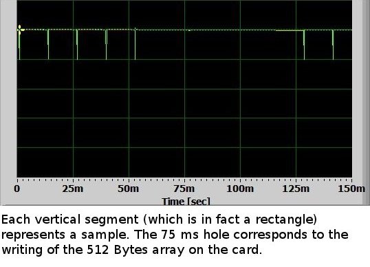
The SDFS library allows choosing if the SPI mode is achieved “by program” or by using the PIC18LF4620 internal functionality (“HardSpi”). But from experience I can say that there is no significant difference. This tends to prove that the slowness is probably more rooted in the file management itself (sector search, answer speed of the card, etc.) than in the only transfer operation itself.
After this, I taken over the code by cutting all non-essential operations and by simplifying the file system management to a minimum and by NOT using partitioned cards. However, although I use exclusively 2 Go cards, and the firmware reads the MBR to allow the use of smaller capacity cards. This does not affect writing operations.
I mainly decompose the writing operation by making the data transfers word by word, as the samples are built up. So, the "write end" of the current 512B sector and the "write initialization" of the following one are assembled in the same time segment, then incompressible (and partly unpredictable ; see further). Those are the limits of the process.
Lastly, the functions of the SDFS library – as with C18 – are multi-files, i.e. are capable to produce and manage as many files as allowed by the FAT16 system. This implies a significant loss of time during the write operations. That is why I limit to only one the number of files recorded on a card, as Carlo Tauraso in his tutorial. This limitation may be embarrassing for long recordings (it is however possible to divide the file afterwards with an hexadecimal file tool as Okteta), but could be resolved only by a radically different way of conception, by separating sampling operations and recording ones, using RAM and two processors. Although I have not attempted to do it, I am sceptical about the possibility to use interrupts to continue sampling during recording periods, because however appealing they may be, our SD cards are rather capricious …
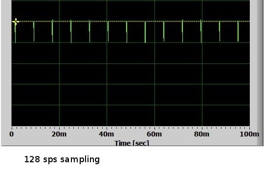
About the SPI implementation “by program”, I point out that the Picbasic Pro has two procedures for reading and writing in the serial synchronous mode, "Shiftin" and "Shiftout". They are perfectly documented in the manual and very easy to use. But if the frequency “of about 50 KHz” of the clock signal which is generated by these procedures, is sufficient for operations as time reading on the RTC or root directory writing, it is not the case for the data recording. The solution is well known : rewrite these two subroutines in assembler without parameter and in the particular case of the ports related to the card. The speed improvement is important and sufficient to sample at 128 sps.
To generate a clock wave on a MCU port, it is very easy : it is sufficient to set the pin successively to 1 and 0 after a delay corresponding to the plateau length of the crenel function establishing the signal. Meanwhile, we send the signals to be transferred by putting the suitable pin to 0 or 1.
To space the samples of the required time to reach the exact sample rate of 128 sps, I use the TIMER0 in 16 bit timer mode (cf. the PIC18F4620 data-sheet p. 123 sqq). The principle of the calculation is :
We start from the crystal frequency, which is 20 MHz ; we deduce the instruction frequency, which is the quarter of it, that is to say 5 MHz, which therefore gives us an instruction cycle duration of 1/(5.10^6) = 0.2 us .
The sampling rate being 128 sps, the duration of a sampling cycle (production of a sample + waiting time before the following) is 1/128 = 7812.5 us.
The production time of a sample depends on the clock signal frequency which is set on the pin 8 of the PIC. If a plateau time corresponding to two instruction cycles (i.e two NOP in Picbasic Pro) is adopted, we have an ADC clock frequency of 5/4 MHz, i.e. 1.25 MHz, which is the double of the maximal frequency allowed (cf. AD7680 data-sheet p. 6) and so, a 24 clocks (4 + 16 + 4) conversion time in 24x4x0.2 = 19.2 us.
Without prescaler, a priori unnecessary here, as it will be seen below, the TIMER0 frequency is 5 MHz ; then, a TIMER0 cycle of 0.2 us. Therefore we must wait for (7812.5 - 19.2)/0.2 ~ 38966 TIMER0 ticks, which remains below the overflow value (65536) in 16 bit mode.
In fact, this calculation undervalues the durations for various reasons. Moreover, the real crystal frequency differs always slightly from its nominal frequency. Instead of attempting to exactly calculate (with mistakes !) the number with which 38966 must be replaced, it is more efficient to proceed by successive approximations by polling the 50(60) Hz line position on waterfalls up to obtain exactly 128 sps. It would be a good thing to achieve a final control by dividing the sample number (half of the file size in bytes) by the duration in seconds of a dozen hours' recording. But, given the sampling time overruns every 256 samples, the total number of samples is slightly inferior to what it should be (cf. infra).
As far as I am concerned, I have to take 37523, which gives the following waiting loop (after TIMER0 reset) :
While TMR0L + 256 * TMR0H < 37523
Do nothing
End While
Do nothing
End While
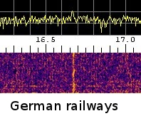
If someone uses without modification my executable file recorder-1.hex, they must determine the exact sampling frequency to fill the field “sample rate” of their FFT tool. He can use a precise function generator or make a recording and try different values until the 50 (60) Hz line approaches as must as possible the corresponding scale graduation on the waterfall. The power frequency measured at my home with a good multimeter generally varies between 49.97 and 50.01 and decreases during the day with the charge of the distribution network. In Europe, we have another reference with the 16.66 Hz ELF waves emitted by the power wires of the German railways, which are received down to central France.
The imperfection of the simplified architecture used here, i.e. without separating the sampling and registering operations is due to the fact that, while the subroutine WRITE_END is performed, every 256 samples, the SD card is polled to know if it is busy or not, the program having to wait until a certain value is non-zero. The problem is that this waiting time may be as long as unpredictable and may overcome the normal time between two samples. In my opinion, this is the cause of the slight instability of the sampling visible at the oscilloscope and of minor relevance. By comparing the counter value at the end of the waiting loop of the busy bit with different cards, I could notice that the card quality had a significant effect. I obtained the best result with the 2 Go Sandisk Ultra cards and I saw that some cheap cards cannot simply be used.
N.B. I tried various prescalers (1:2, 1:4, 1:8) in the hope of avoiding reaching the TIMER0 overflow whereas the recording of the 512B block is not achevied, and thus stupidly prolonging stupidly a labs time already too long. It seems at the oscilloscope that the result would be slightly better, some overruns being less important, but the quantum of time being greater, it is impossible to obtain a sample rate of exactly 128 sps (even without prescaler). Ultimately, I did not use any prescaler (so, I obtain 127.85 sps), but if anyone wants to try one, the values to use are commented on in the source file.
It is impossible to tell more about the program on this site without abusing our friend Renato's hospitality, but it is possible to write to me to have clarifications and further information. However, I would like to say a few words in annex about the mysterious CRCs although they are little used here (Annex about CRCs).
Practical considerations
The present work can be used at various levels according to one's own knowledge and experience about microcontrollers (MCUs). People unfamiliar with MCUs will first have to acquire the basics of them, at least with regard to the Microchip PIC18s. In all cases, it is necessary to have a serial port on one's PC and a good serial port tool being able to transmit in STRING, DEC and HEX. I use with satisfaction Advanced Serial Port from Eltima Software after I tried various free applications which did not work properly (that does not mean that good ones do not exist).
- Minimalistic solution
* Buy a Pickit2 programmer ref. PG164120 (or Pickit3, but the Pickit2 is sufficient and cheaper) and install on a PC MPLAB after downloading from the Microchip Website for free. If it is not envisaged modifying the source file, it is sufficient to use the simple programming software supplied with the Pickit2.
* Download here the executable file recorder-1.hex.

* Plug the Pickit2 (linked to the PC with its USB connector) into the 6 pin ICSP male connector and program the PIC18LF4620 after correctly parametrizing the programming software (or MPLAB) and loading the hex file. Be careful not to confuse Vcc (or Vdd, here 3.3V) and Vpp, which is the programming voltage (about 13V), provided by the Pickit2 via the USB connector. The Vcc voltage, necessary during the programming time can be supplied by the Pickit2 or by the system power supply, which then may be turned on. In the first case it is better that the SD card be removed from its connector to limit the current provided by the USB plug.
Take care NOT to tick the box “Preserve EEPROM”, otherwise the file name “RECORD.DAT” will not be written on the card. In return, it is necessary to set the recording time after each programmation. Remove the Pickit from the ICSP connector after cutting off the Vdd on MPLAB in the "programmer" menu.
* After a few seconds' rest period, the recorder is ready for use. Firstly, it must be parametrized. To do so, connect the serial wire between the PC and the recorder, launch the RS232 tool and open a session (baudrate : 9600 Bds, data bits : 8, parity : none, stop bits : 1, flow control : none). The recorder being not powered, press and maintain the “SET” button down, then press the “ON” button. The parametrization dialogue must appear on the screen. Set the time and establish the required recording duration. Quit. The system is ready for use.
* Recording is launched by pressing a few seconds the “REC. ON” button. If it is necessary to stop it before the programmed time, just press a few seconds the button “REC. OFF” until the green led turns off. Then, the file is properly closed and it is possible to remove the SD card.
* If, unfortunately, the red led, announcing a recording error, turns on unexpectedly as soon as the “ON” button is pressed, maintain the “RESET” button down a dozen seconds after pressing the “OFF” button. This may indicate a partial deterioration of the MCU and it would be advisable to try again with a new one if the phenomenon becomes recurring.
* The system has no battery monitoring. It would have been very easy to add one, by using the on-chip ADC of the PORTA for instance. I have not done so in order not to overload the processor during a critical moment and mainly because I think it is unnecessary. In fact, it is recommended not to discharge the LSA batteries beyond about a third of their capacity and recharge them immediately after use.
- SD card formatting
It is important to use brand-name cards and not to skimp on a few cents because some cheap cards have an erratic behaviour in SPI mode.
As said before, they must be formatted in plain FAT16 and WITHOUT PARTITION. As it is visible in the FAT16 specifications, for 2 GB cards, we have 512B sectors and 64 sector clusters (i.e. 32 KB clusters).
I am showing you how I proceed to format my SD cards :
1°/ With the free partition editor Gparted (which runs under Windows or Linux) : select the medium (be careful not to target the HDD, which is selected by default).
Then : Device → Create → Partition table → Advanced → Loop → Apply.
2°/ Under Linux : sudo mkdosfs -I -F 16 /dev/sdd. Under Windows 7 use the integrated formatting tool : FAT, allocation unit (cluster size) : 32 KB. It is also possible to use the Panasonic SD Formatter.
- Exploitation of results
With Spectrum Lab : File → Audio Files → Analyse Audio Files (without DSP), …
With Baudline : right click → Input → Open File → Raw → Open → Decompression OFF, Initial byte : 0, Sample rate : custom, 128, 16bit linear, little endian.
- Date and hour
For the convenience of archiving, the file names are automatically stamped with the date and the time of the beginning of the recording in the following format (on 8 characters) : MMDDHHMM.DAT. There is no place for the year ...
- Hardware
I must indicate that I firstly made a development board before the definitive one. I used stripboard, except for receiving the SD card socket for which I was forced to realize a true small PCB. To make such small PCBs I draw the copper zones with Libre Office Draw (without inversion), I print the drawing with a laser printer on photo paper for inkjet printer (HP Everyday semi-glossy) and I transfer the ink on the copper clad board with an iron set at the maximum temperature. Before the transfer, the board must be frosted with a clean Scotch-BriteTM, perfectly defatted and without finger mark. After cooling, I delicately remove the paper after soaking in water and I corrode the copper to be removed, with hydrochloric acid added with a little 130 volume hydrogen peroxide.
As PC oscilloscope, I used with satisfaction (http://www.zeitnitz.de/Christian/scope_en), which is free for a non-commercial use. However the sample rate of the sound card does not allow seeing the bits of the samples separately.
Return to www.vlf.it main index